

Ultra-scalable photonics for quantum computing and networking
High-speed programmable photonic integrated circuits
This research project aims to develop high-speed programmable photonic circuits compatible with cryogenic temperatures and use a complementary metal-oxide-semiconductor (CMOS) fabrication process architecture for the visible-near infrared spectrum.
Recent advances in photonic integrated circuits (PICs) technology that uses light to perform various functions found their use in applications for computation, communication, and sensing. They are essential development because they allow for integrating multiple optical components onto a single chip, leading to smaller, more efficient, and more versatile devices. One of the most critical components of PICs is Mach-Zehnder interferometers (MZIs).
MZIs are interferometers that use two parallel beams of light to interfere with each other. When these MZIs are cascaded, they form a Mach-Zehnder mesh (MZM), which can perform universal linear-optical transformations on N input/output optical modes. MZMs serve critical functions in photonic quantum information processing, quantum-enhanced sensor networks, machine learning, and other applications. We introduce a large-scale MZM platform made in a 200 mm complementary metal–oxide–semiconductor foundry, which uses aluminum nitride piezo-optomechanical actuators coupled to silicon nitride waveguides, enabling low-loss propagation with phase modulation at greater than 100 MHz in the visible–near-infrared wavelengths. Moreover, the vanishingly low hold-power consumption of the piezo-actuators enables these photonic integrated circuits to operate at cryogenic temperatures, paving the way for a fully integrated device architecture for a range of quantum applications [1-2].
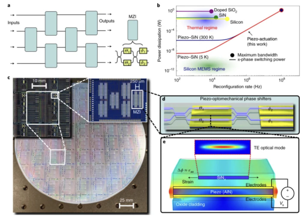
a, Schematic of a four-mode programmable circuit consisting of cascaded MZIs for SU(4) operations. b, Trade space diagram of the power–reconfiguration rate for other CMOS-compatible photonic technologies and our piezo-actuated photonics. c, Microscopy images of a fully processed 200 mm wafer with insets showing the zoomed-in view of a reticle and a 4 × 4 MZM. d, Three-dimensional concept art of an MZI with piezo-optomechanical phase shifters. e, Cross-sectional diagram of our phase shifter, illustrating how an applied voltage across the piezo results in strain imparted to the optical waveguide.
References
[1] High-speed programmable photonic circuits in a cryogenically compatible, visible–near-infrared 200 mm CMOS architecture, Nature Photonics volume 16, pages 59–65 (2022).
[2] High-fidelity trapped-ion qubit operations with scalable photonic modulators, arXiv: 2210.14368 (2022).
Atom-control photonic integrated circuit (APIC) platform
Advancement in the laser technology has driven discoveries in atomic, molecular, and optical (AMO) physics and emerging applications, from quantum computers with cold atoms or ions to quantum networks with solid-state color centers. This progress is motivating the development of a new generation of “programmable optical control” systems, characterized by criteria,
1. visible (VIS) and near-infrared (IR) wavelength operation,
2. large channel counts extensible beyond 1000s of individually addressable atoms,
3. high-intensity modulation extinction,
4. repeatability compatible with low gate errors,
5. fast switching times.
We are addressing these challenges by introducing an atom control architecture based on VIS-IR photonic integrated circuit (PIC) technology. Based on a complementary metal-oxide-semiconductor (CMOS) fabrication process, this Atom-control PIC (APIC) technology meets the system requirements 1-5.
As a proof of concept, we have demonstrated a 16-channel silicon nitride-based APIC with (5.8\pm±0.4) ns response times and -30 dB extinction ratio at a wavelength of 780 nm [1].
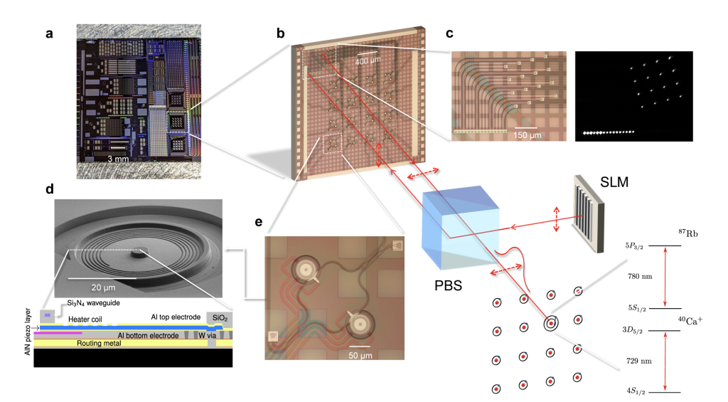
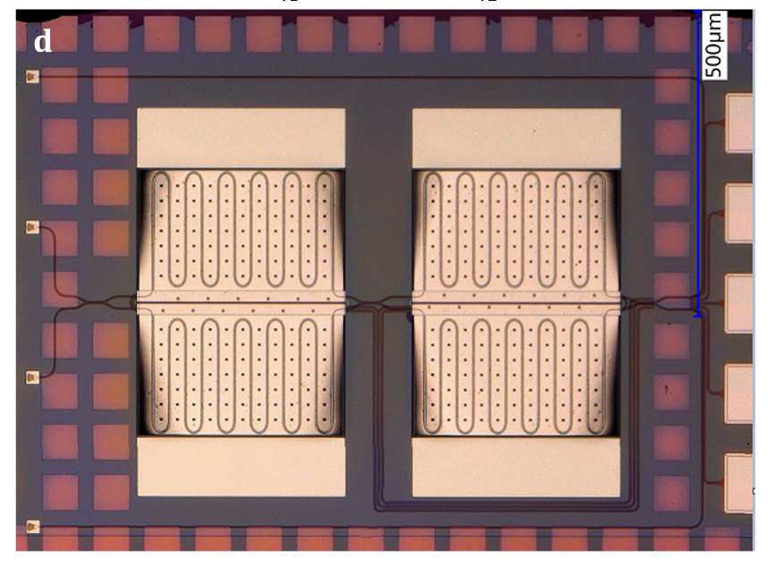
Atom-control photonic integrated circuit (APIC) platform. a, Photograph of the full reticle. b, APIC modulator array with a modulator pitch of 420µm. c, 4×4 out-coupling and 1×16 in-coupling area. Chip detail (left) and camera image with light coupled into all ports (right). d, SEM image of the individual ring (top). Schematic cross-section of the device with piezo-stack and waveguiding layers illustrated. e, DRMZM with local in- and out-coupling gratings can be used as an alternative to the grating couplers in c. Bottom right: Illustration of setup. An SLM projects light onto the APIC, where the light is modulated and after passing through a PBS imaged onto an array of (artificial) atoms.
References
[1] Scalable photonic integrated circuits for programmable control of atomic systems, arXiv:2210.03100 (2022).
Piezo-Optomechanical Integration of Diamond Emitters
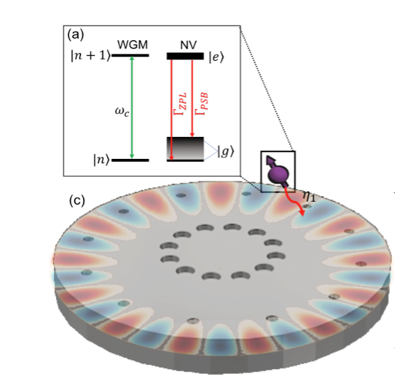
A leading qubit candidate for ultra-scalable quantum computing and networking is the solid state spin qubit hosted in point defects in diamond. These defects, known as color centers (CCs), have optically addressable transitions, allowing for optical initialization and readout, as well as long spin qubit coherence times, with even longer coherence times by coupling to nearby nuclear spins [1]. By implanting CCs in diamond microdisk resonators [2], collection efficiency of the CC photons can be enhanced. However, in order to perform quantum gates on CCs with scalable platforms like photonic integrated circuits (PICs), it is necessary to develop an efficient method of interfacing between CCs and PICs. We are addressing this challenge by developing a piezo-optomechanical PIC quantum socket that allows for MEMS-enabled control of all optical and spin degrees of freedom of heterogeneously integrated CCs in diamond microdisk resonators. These degrees of freedom include:
- Zero-phonon-line (ZPL) frequency of the emitted photon, controlled through static piezoelectric strain tuning [3, 4];
- Frequency of the diamond microdisk cavity mode, controlled through evanescent dielectric perturbations;
- Coupling rate between the diamond microdisk cavity and the PIC waveguides, controlled through interferometric coupling and a piezoelectric phase shifter [5];
- Electronic and nuclear spin control through dynamic strain by exciting a mechanical eigenmode of the microdisk resonator [6, 7].
References
[1] Stas, P.-J., et al. Robust multi-qubit quantum network node with integrated error detection. Science, vol. 378, no. 6619, pp. 557–560, (2022).
[2] Duan, Y., Chen, K.C., et al. A Vertically Loaded Diamond Microdisk Resonator (VLDMoRt) towards a Scalable Quantum Network. Conference on Lasers and Electro-Optics (CLEO) (2021), paper JW4L.6.
[3] Meesala, S., et al. Strain engineering of the silicon-vacancy center in diamond. Phys. Rev. B, vol. 97, p. 205444, (2018).
[4] Clark, G., et al. Nanoelectromechanical Control of Spin–Photon Interfaces in a Hybrid Quantum System on Chip. Nano Lett. 2024, 24, 4, 1316–1323 (2024).
[5] Dong, M., et al. Piezo-optomechanical cantilever modulators for VLSI visible photonics. APL Photonics (2022).
[6] Maity, S., et al. Coherent acoustic control of a single silicon vacancy spin in diamond. Nat Commun 11, 193 (2020).
[7] Maity, S, et al. Mechanical control of a single nuclear spin. Phys. Rev. X 12, 011056 (2022).
High-fidelity trapped-ion qubit operations with scalable photonic modulators
Ion-trapping technology has matured to the point that traps are being microfabricated on chips, like the Phoenix trap at Sandia National Laboratories.
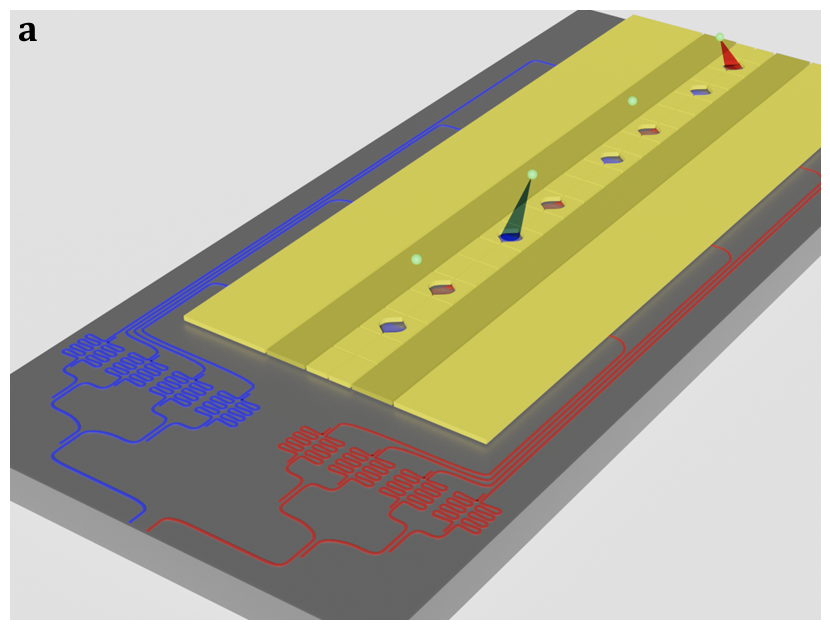
Calcium ions contain a 2-level system with a transition driven by 729 nm light which can function as a qubit. These trapped-ion quantum computers require precise optical modulation in order to drive the transitions of the ions and thus perform gate operations on the qubits. The focus of our group is on the optical control and its scalability. Since every qubit requires a unique optical signal, producing beams off-chip and edge-coupling them with fibers quickly becomes unsuitable because the number of ions can grow as the area of the chip while the edge-coupling I/O grows with its perimeter. The solution is to input a single optical signal onto the chip and then split the light with waveguide beamsplitters into the desired number of separate channels which are then individually modulated by an electrical signal.
Our group has produced a device employing the aforementioned approach using piezoelectrically actuated Mach-Zender modulators (MZMs).
The MZMs consist of a waveguide layer acting as two Mach-Zender interferometers, which sit above a piezoelectric substrate sandwiched between electrodes. When voltage is applied to the electrodes, the piezo-material is strained which in turn strains the waveguide and produces a change in phase along one of the waveguide-arms relative to other. In this way the signal entering the MZM can be amplitude modulated as a function of the voltage applied to the electrodes. Computational gates (rotations about the X and Y axes of the Bloch sphere) and the identity gate implemented with one of these MZM-based devices yielded gate-fidelities exceeding 99.7%. These results show that the modulators perform on-par with the state of the art and in principle can scale with the number of qubits needed for true, large-scale trapped-ion quantum computers.
References:
[1] High-fidelity trapped-ion qubit operations with scalable photonic modulators, C. W. Hogle, D. Dominguez, M. Dong, A. Leenheer, H. J. McGuinness, B. P. Ruzic, M. Eichenfield, and D. Stick1, arXiv:2210.14368 2022.