Quantum phononics
Phonons are quantized units of acoustic energy and are analogous to photons in the electromechanical regime. This allows us to draw inspiration from work done in quantum photonics while we work to develop a quantum phononics platform built around acoustoelectric devices. Placing a thin film semiconductor or a 2D electron gas (2DEG) on top of a piezoelectric material hybridizes the phonons with electromagnetically driven, overdamped electronic waves in the semiconductor, leading to a greatly enhanced phononic nonlinearity. This nonlinearity is several orders of magnitude larger than the nonlinearity found in bulk piezoelectric semiconductors, allowing for the development of novel integrated phononic devices that can operate in the quantum regime. Current work is focused on developing parametric amplifiers and nonlinear phononic cavities.
Parametric amplifiers are critical devices in quantum systems as they allow for amplification of sensitive quantum signals. Without parametric amplifiers, it can be difficult to read out quantum signals without introducing too much noise and destroying your measurement in the process. Such devices have been developed in traditional superconducting systems with the use of Josephson junctions [1].
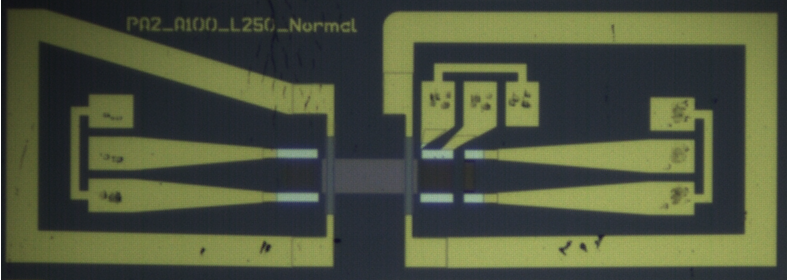
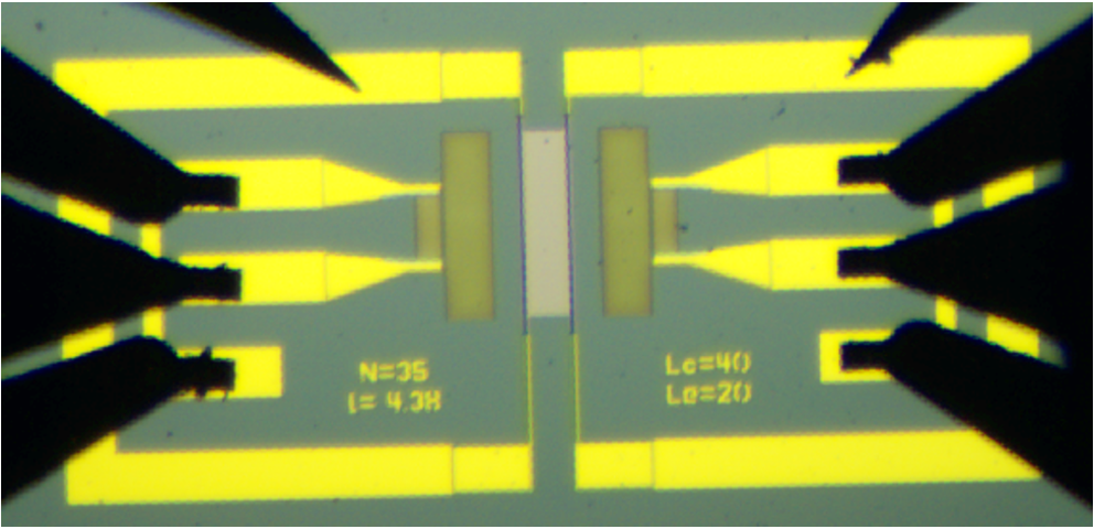
Pictured below is an example of a room temperature device constructed by placing a bulk semiconductor on top of lithium niobate. Through the piezoelectric response of lithium niobate, we can excite acoustic waves by utilizing Inter-Digitated Transducers (IDTs). This same piezoelectric response allows the acoustic wave to interact with the free electrons in the semiconductor layer, which introduces a greatly enhanced acoustic nonlinearity. This allows us to develop nonlinear devices such as parametric amplifiers and develop novel quantum acoustoelectric devices.


References:
[1] C. Macklin et al., A near–quantum-limited Josephson traveling-wave parametric amplifier. Science350,307-310(2015).DOI:10.1126/science.aaa8525
[2] E. Chatterjee, A. Wendt, D. Soh, and M. Eichenfield, “Ab initio calculations of nonlinear susceptibility and multiphonon mixing processes in a 2DEG-piezoelectric heterostructure,” Physical review research, vol. 6, no. 2, Jun. 2024, doi: https://doi.org/10.1103/physrevresearch.6.023288.
Strain tuning of solid-state defects
Solid state defects are one of the leading platforms for both on-demand single photon emitters as well as optically accessible quantum memories [1- 2]. While there have been numerous demonstrations of individual spin control and deterministic single photon sources from a single device, scaling these devices remains challenging. Local environmental differences lead to perturbed electronic structures, causing defects to emit at slightly different frequencies.
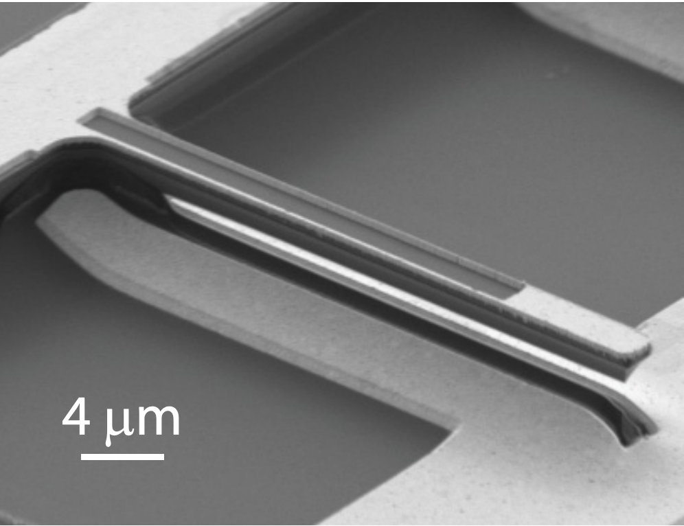
Strain tuning, the process of modifying the electronic structure of a point defect through the application of static strain, is the most natural approach to tune these centers [3]. This approach provides a clear pathway to creating
large arrays of indistinguishable emitters.

References:
[1] P.-J. Stas, Y. Q. Huan, B. Machielse, E. N. Knall, A. Suleymanzade, B. Pingault, M. Sutula, S. W. Ding, C. M. Knaut, D. R. Assumpcao, Y.-C. Wei, M. K. Bhaskar, R. Riedinger, D. D. Sukachev, H. Park, M. Lonˇcar, D. S. Levonian, and M. D. Lukin, “Robust multi-qubit quantum network node with integrated error detection,” Science, vol. 378, no. 6619, pp. 557–560, 2022.
[2] L. Komza, P. Samutpraphoot, M. Odeh, Y.-L. Tang, M. Mathew, J. Chang, H. Song, M.-K. Kim, Y. Xiong, G. Hautier, and A. Sipahigil, “Indistinguishable photons from an artificial atom in silicon photonics,” 2022.
[3] S. Meesala, Y.-I. Sohn, B. Pingault, L. Shao, H. A. Atikian, J. Holzgrafe, M. G ̈undo ̆gan, C. Stavrakas, A. Sipahigil, C. Chia, R. Evans, M. J. Burek, M. Zhang, L. Wu, J. L. Pacheco, J. Abraham, E. Bielejec, M. D. Lukin, M. Atat ̈ure, and M. Lonˇcar, “Strain engineering of the silicon-vacancy center in diamond,” Phys. Rev. B, vol. 97, p. 205444, May 2018.

