
Research: Nanomanufacturing Using Optical Tweezers
Optical tweezers use focused laser beams to pick up, move, and place microscale and nanoscale objects. We have created a computer-controlled nanomanufacturing platform based on optical tweezers. A current challenge in this field is how to construct three-dimensional (3D) structures out of multiple types of materials with feature sizes less than 100 nanometers.
Optical Positioning and Linking (OPAL)
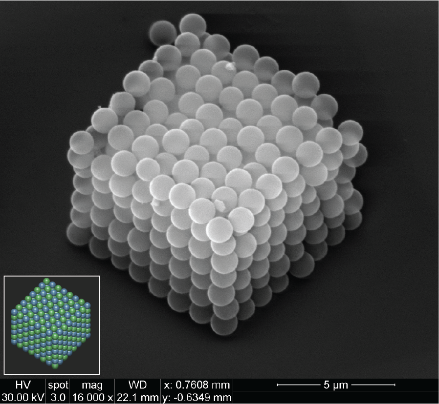
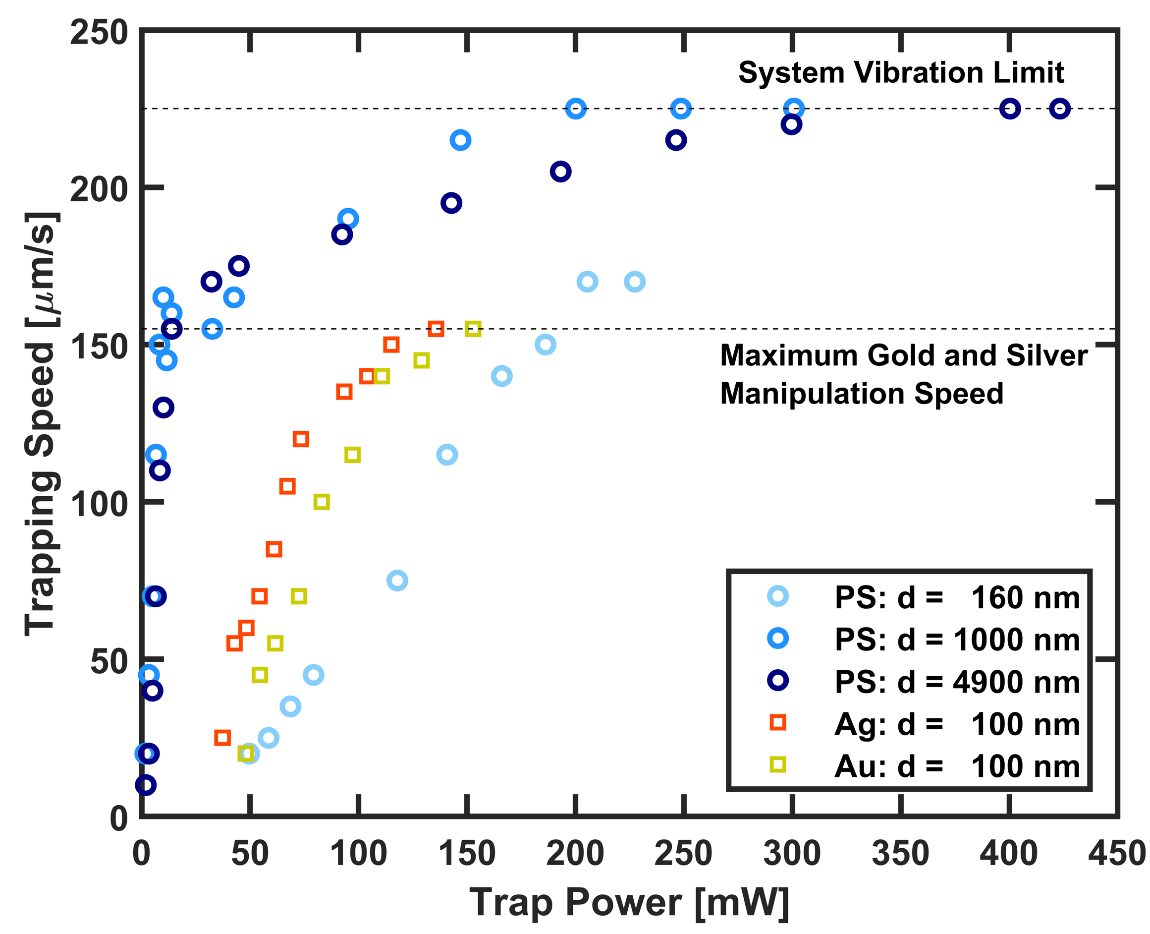
Many of the most exciting photonic applications, such as superlensing or cloaking, rely on components much smaller than the wavelength of light to provide exotic optical properties like a negative refractive index or a refractive index near zero. Such properties cannot be found in “natural” homogeneous materials. We are using optical tweezers to fabricate complex 3D arrangements of nanoparticles that are linked using chemical bonds. We have demonstrated some of the fastest published optical tweezer manipulation speed for nanoparticles, which is significant because manipulation speed can be the limiting factor in how long it takes to assemble devices. We have also discovered that a widely-used skin-depth correction factor for calculating the optical trapping strength of metallic nanoparticles is rather inaccurate, and we have provided a better alternative. We use a custom implementation of the discrete dipole approximation algorithm to simulate and design nanophotonic materials and devices. At the microscale, we have assembled more than 440 building blocks in a continuous rigid cubic structure, demonstrating the precision and repeatability of our automated assembly platform.
A few relevant articles include (see publications for all related articles):
- Weilin Liu and Euan McLeod, “Fast and accurate electromagnetic field calculation for substrate-supported metasurfaces using the discrete dipole approximation,” Nanophotonics, 12 (22), 4157-4173 (2023).
- Jeffrey E. Melzer and Euan McLeod, “Assembly of multicomponent structures from hundreds of micron-scale building blocks using optical tweezers,” Microsystems & Nanoengineering, 7, 45 (2021).
- Jeffrey E. Melzer and Euan McLeod, “Fundamental limits of optical tweezer nanoparticle manipulation speeds,” ACS Nano, 12, 2440 (2018).
- Jeffrey E. Melzer and Euan McLeod, “3D Nanophotonic Device Fabrication Using Discrete Components,” Nanophotonics, 9 (6), 1373-1390 (2020).
- Weilin Liu and Euan McLeod, “Accuracy of the skin depth correction for metallic nanoparticle polarizability,” Journal of Physical Chemistry C, 123 (20), 13009-13014 (2019).
Nano-Enhanced Whispering Gallery Mode Sensors
We are collaborating with Prof. Judith Su’s Little Sensor Lab and Prof. Brian Stoltz’s group at Caltech to create enhanced chemical and biological sensors based on microtoroidal optical resonators augmented with photonic nanostructures. Silica microtoroids, typically ~100 μm in diameter, guide light within themselves due to total internal reflection. They exhibit resonances when their circumference equals an integer number of wavelengths. Some of the light is guided evanescently outside of the microtoroid and interacts with the surrounding environment. This interaction usually slows down the light, shifting the resonance wavelength. By tracking these shifts, microtoroidal optical resonators can be used as very sensitive sensors.
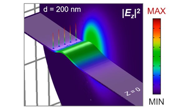
The sensitivity of the sensors can be further enhanced by attaching nanoparticles to the rim of the microtoroid, which provide a stronger interaction between the light and the environment than that of a bare microtoroid. Precisely-engineered nanostructures can also be used to couple light in and out of the microtoroid, providing a more robust alternative to the fragile and vibration-sensitive tapered optical fibers that are most commonly used for coupling. We have developed new numerical techniques to design such nanostructures and we are attaching them to microtoroids using OPAL.
A few relevant articles include (see publications for all related articles):
- Sartanee Suebka, Euan McLeod, and Judith Su, “Ultra-high-Q free space coupling to microtoroid resonators,” Light: Science & Applications, 13, 75 (2024).
- Yinchao Xu, Allison Stanko, Chloe Cerione, Trevor Lohrey, Euan McLeod, Brian Stoltz, and Judith Su, “Low Part-Per-Trillion, Humidity Resistant Detection of Nitric Oxide Using Microtoroid Optical Resonators,” ACS Applied Materials & Interfaces, 16 (4), 5120-5128 (2024).
- Cheng Li, Trevor Lohrey, Phuong-Diem Nguyen, Zhouyang Min, Yisha Tang, Chang Ge, Zachary Sercel, Euan McLeod, Brian Stoltz, and Judith Su, “Part-per-trillion trace selective gas detection using frequency locked whispering gallery mode microtoroids,” ACS Applied Materials & Interfaces, 14 (37), 42430-42440 (2022).
- Lei Chen, Cheng Li, Yu-min Liu, Judith Su, and Euan McLeod, “Simulating robust far-field coupling to travelling waves in large three-dimensional nanostructured high-Q microresonators,” Photonics Research, 7 (9), 967-976 (2019).
- Cheng Li, Lei Chen, Euan McLeod, and Judith Su, “Dark mode plasmonic optical microcavity biochemical sensor,” Photonics Research, 7 (8), 939-947 (2019).
Optical Trap Assisted Nanopatterning
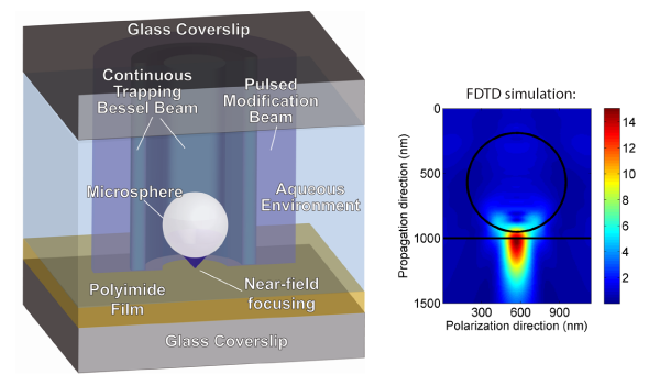
In a previous project, which we are not currently working on, we developed an optical trap-assisted nanopatterning (OTAN) technique. In OTAN, an optical trap is used to position a dielectric sphere within a few tens of nanometers of a surface. This sphere is used as a near-field focusing objective to directly write sub-diffraction-limit features that are smaller than 100 nm onto a surface using a laser. This maskless lithography technique could be used to fabricate devices that would otherwise require electron-beam lithography or deep-UV lithography. In our approach, the feature size of 100 nm is smaller than one-third the laser wavelength (355 nm). To achieve these results we use a specialized optical trap based on a Bessel beam, which facilitates the repeatable patterning of rough, tilted, or curved surfaces.
A few relevant articles include (see publications for all related articles):
- Euan McLeod and Craig B. Arnold, “Array-based optical nanolithography using optically trapped microlenses,” Optics Express, 17 (5), 3640-3650 (2009). Featured in Nature Photonics, 3, 261 (2009).
- Euan McLeod and Craig B. Arnold, “Subwavelength direct-write nanopatterning using optically trapped microspheres,” Nature Nanotechnology, 3, 413-417 (2008).