
QD/QW growth via MBE for incorporation of nanocavities
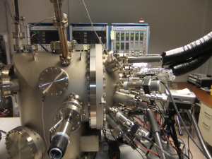
MBE Facilities
We use a Riber 32P MBE (molecular beam epitaxy) system for the growth of InGaAs/GaAs, GaAs/AlGaAs, GaAlInAs structures. The Riber 32P has three chambers. The ion-pumped load chamber includes a unit for the prebaking of moly blocks and samples (wafers up to 3″). The chamber for growing samples contains gallium (Ga), arsenic (As), indium (In), and aluminum (Al) effusion cells, RHEED analysis, and a quadrupole mass analyzer. The temperatures of the cells are maintained by feedback control; shutter actuations are computer controlled.
What is MBE?
MBE, or molecular beam epitaxy, is essentially a method of growing materials one layer of atoms at a time. A substrate (in our case, a semiconductor wafer) is placed in an ultra-high vacuum. Our MBE machine operates at about 1E-12 torr. This is about the same molecular density as the earth’s atmosphere at the altitude of the International Space Station. The substrates are then baked out to remove any contaminants (especially residual water molecules) on the surface. Once the substrate is prepared, layers of desired atoms are placed on the substrate one at a time. This is done by heating the effusion cells (these contain the materials we wish to place on the substrate), which causes atoms to “evaporate” out of the effusion cells and stream towards the substrate. By controlling which effusion cells are active at a given time, as well as how long an effusion cell is active, it is possible to control the thickness of the layer placed on substrate. This makes it possible to custom-engineer semiconductor structures such as quantum wells and microcavities. The thickness of a layer is generally not constant across the entire wafer. The stream of atoms leaving an effusion cell deposits onto the substrate most quickly at the center of the stream. The point on the substrate that coincides with the center of the stream is called the growth center. As one moves away from growth center, the thickness of the layer decreases. The thickness of the layer at a given point must be an integer number of atoms. Therefore, the layer’s thickness decreases in integer steps of atomic width. Since deposition is a random process, these steps usually do not occur along a well defined line. Instead the tendency is that islands and wells will form, in which the layer is one atom thicker or thinner than surrounding the island or well. Since the electron excitation energy is dependent on the layer width, these islands and wells act as quantum mechanical finite wells and barriers (not necessarily square). This gives rise to interface fluctuation quantum dots. One of our current areas of research is determining the growth conditions that give rise to well-defined interface fluctuation quantum dots.