
Coupling Metal Nanocavities to Semiconductor QWs/QDs
While traditional dielectric optical cavities are limited in size by (λ/n)3, metallic nano-cavities can have volumes on the order of 1000 times smaller than this. This sub-wavelength size leads to a large enhancement of the local density of states which can significantly alter the emission properties of nearby active material. In particular we are interested in the resonant coupling of these nano-cavities to semiconductor quantum wells and quantum dots.
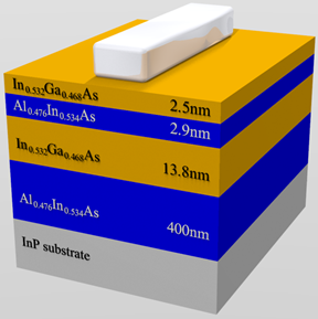
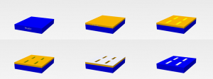
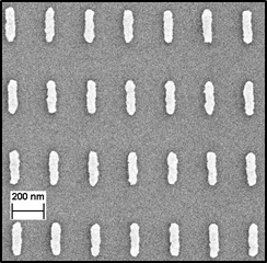
After quantum well/dot samples are grown by molecular beam epitaxy, arrays of metallic nano-cavities are fabricated on the surface. Using electron beam lithography, patterns of metallic cavities are written into a PMMA resist layer. After developing this layer the sample is coated with a 30nm film of high purity silver. Using a solvent the PMMA layer is dissolved. Excess silver floats away, leaving behind the silver cavities.
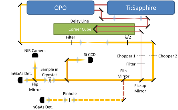
In order to measure the effect of these cavities on the underlying semiconductor we perform time resolved pump-probe spectroscopy. The semiconductor is pumped using a Ti:Sapphire laser with 120 fs pulses, while a separate probe pulse measures the resulting change in transmission of the sample. The probe pulse is passed through a variable delay line, allowing the observation of the temporal dynamics. Additionally, the probe is tunable from 1360nm to 1580nm allowing spectral resolution.